Chip design in the semiconductor industry is an essential part of modern electronics. This process plays a crucial role not only in creating fundamental electronic components but also in shaping advanced technology products such as mobile phones, computers, and IoT devices. Let’s delve deeper into Semiconductor Chip Design and the design process with FPT Jetking.
What is Chip Design in the Semiconductor Industry?
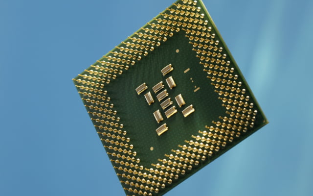
Chip design in the semiconductor industry involves designing and developing integrated circuits based on semiconductor materials like silicon to create electronic components such as processors, memory chips, logic circuits, and other components. This process includes designing electronic circuits, simulation, verification, and manufacturing semiconductor chips. Semiconductor Chip Design is critical in creating technological products like mobile phones, computers, consumer electronics, and many other industrial applications.
Chip Design Flow

Functional Design
After identifying requirements and specifications, the next step is functional design. This process focuses on defining the chip’s functionality and behavior. It involves creating a high-level description of system requirements and designing algorithms and data flows to meet these requirements. The goal of this phase is to produce a detailed functional specification that can be used as a basis for the subsequent design phases.
Logic Design
This step focuses on creating the digital logic circuits needed to implement the functions defined in the functional design phase. This process involves using Hardware Description Language (HDL) to create logic designs and simulation to verify the accuracy of the design.
Circuit Design
In this stage, the physical circuits of the chip are designed, including the selection and placement of components like transistors, resistors, capacitors, and other elements. The power and clock distribution networks are also designed during this phase.
Physical Design Verification
This process involves checking the physical layout of the chip to ensure it meets design requirements and will be accurately manufactured. EDA software tools like logic simulation and logic analysis are used to check the integrated circuit layout design.
Verification and Validation
After the design is completed, verification and validation are conducted to ensure the chip meets the requirements and functions correctly. This includes testing the chip through various simulation platforms to ensure its accuracy.
Fabrication
Finally, after design and testing, the .GDS file is sent to the foundry for chip fabrication. Each stage of the chip design process is crucial for creating a well-functioning product that meets customer requirements. Understanding each phase helps designers create effective, reliable, and cost-efficient designs.
The Future of Chip Design in the Semiconductor Industry

The future of chip design in the semiconductor industry is exciting and rapidly evolving as technology advances. Next-generation chipsets support modern solutions by providing higher performance, lower power consumption, and enhanced functionality. These advancements drive innovation across many industries.
For example, next-generation chipsets support emerging solutions like Artificial Intelligence (AI) and Machine Learning (ML). AI and ML require significant computing power, achievable with advanced chipsets. These technologies are used to create autonomous vehicles, personalized healthcare solutions, and advanced robotics, among other innovations.
Another area where next-generation chipsets are making a significant impact is the Internet of Things (IoT) space. The proliferation of connected devices requires powerful, energy-efficient, and cost-effective chipsets to enable communication and data processing across a variety of devices. Next-generation chipsets are also advancing 5G networks, expected to provide high-speed connectivity, low latency, and open new possibilities in fields like virtual reality, augmented reality, and remote surgery.
The future of chip design is bright, and next-generation chipsets will offer even more innovative solutions across various industries. As technology evolves, we can expect exciting developments in chip design and the solutions they enable.
In summary, the chip design process is complex and involves multiple steps and stages, having a significant impact on the industry. With many types of chips in use today and new technologies continuously emerging, there will always be opportunities for improvement in how we build these chipsets.
In today’s context, chip design in the semiconductor industry is not only a technological field but also at the core of societal progress and development. By understanding its concepts and design process, we can see the appeal and potential of this industry in the future. It is not only the foundation for technological advancements but also a driving force for creating innovations and new applications in everyday life.
At FPT Jetking, we are open for enrollment in the Semiconductor VLSI Design program, which lasts 2 years and is divided into 4 semesters. The tuition is paid per semester, and the number of payments remains unchanged from the start to the end of the course. Therefore, if you are a student, recent graduate, or professional looking to enhance your knowledge and skills in the field of science and technology in the digital age, please register with FPT Jetking so we can provide you with the fastest consultation possible!